


Advanced Materials and Devices Laboratory
Prof. Satoshi MORIYAMA
![]() Electronic Devices
Electronic Devices![]() Electronic, Information Systems
Electronic, Information Systems
Development of Novel Devices using Advanced Materials for Electronics
In our laboratory, we study electrical properties in two-dimensional atomic-layer materials and advanced silicon quantum devices as shown below.
(1) Electronic properties and device applications of atomic-layer materials
Graphite, a familiar material used for pencil leads, is a layered material consisting of sheets of carbon atoms (graphene). Recently, two-dimensional atomic-layer materials such as transition metal dichalcogenides (TMDC) and hexagonal boron nitride (hBN) as well as graphene have been discovered, and they are the attractive materials for building blocks of state-of-the-art electronics. We aim to realize high-performance electronic and optical devices, memory devices, and topological quantum devices by extracting one layer of atoms and creating artificial atomic layers, which do not exist in nature, by stacking various atomic layer materials like Lego blocks.
(2) Silicon quantum devices
We propose and demonstrate high-temperature operable quantum dots (QDs) and electron-spin qubits based on silicon-on-insulator (SOI) tunnel field-effect transistors (TFETs) with deep levels. We observed single-electron transport through the implantation-induced atomic-size QDs embraced in TFETs up to room temperature. Furthermore, double-QD devices were operated as spin qubits. These results indicate that spin qubits in SOI-TFETs have advantages in realizing the high-temperature operation of quantum computing with established silicon technology.
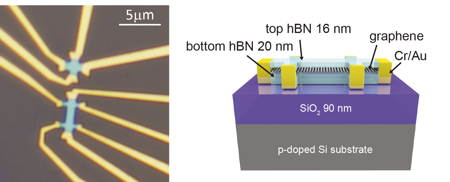
Fig.1: hBN/graphene superlattice device.
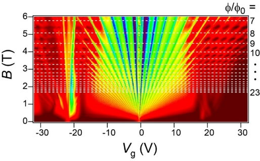
Fig.2: Quantum transport in hBN/graphene supperlattice device.
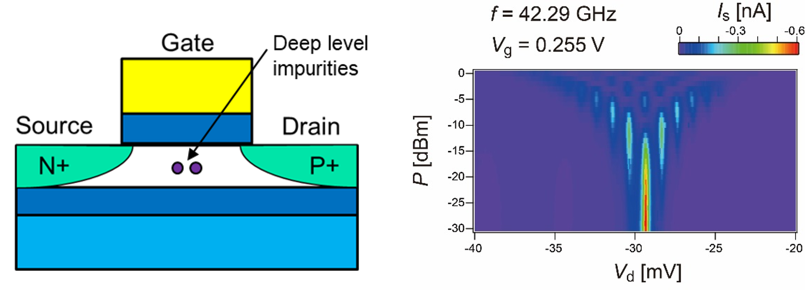
Fig.3: TFET-based qubits.